Jun 11 2021
什么是已经为无机半导体建立的对它们的有机同行仍然是一个挑战 - 也就是说,通过混合各种半导体分子来改善设备的性能来调整能量差距。
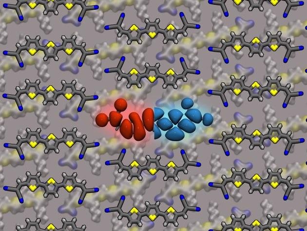 在混合物中改变3T分子(前景)和6T分子(在背景中指示)的比率可以连续调整间隙。图片来源:技术大学德累斯顿。
Researchers fromTechnischeUniversitätDresden(Tu Dresden),与慕尼黑大学的科学家合作,Würzburg大学,胡柏林和乌尔姆大学(Ulm University)现在已经演示了如何实现这一目标。
Organic semiconductors have gained a reputation as energy-efficient materials in organic light-emitting diodes (OLEDs) that are used in large-area displays. In these and other kinds of applications, like solar cells, a major parameter is the energy gap that exists between electronic states.
该能量差距确定产生或吸收的光的波长。实际上,该能量差距的恒定调整是首选。事实上,无机材料已经存在一种合适的技术 - 所谓的混合。亚博网站下载该技术基于通过更换材料中的原子来设计带隙。这可以使恒定的可调性如在砷氧化铝半导体中所致。
Regrettably, this cannot be transferred to organic semiconductors due to their different physical properties and their molecule-based construction paradigm; therefore, this makes constant band gap tuning much more complicated.
But with their new publication, the researchers from the Center for Advancing Electronics Dresden (cfaed, TU Dresden) and from the Cluster of Excellence “e-conversion” at TU Munich along with associates from the University of Würzburg, HU Berlin, and Ulm University realized energy-gap engineering for organic semiconductors by blending, which represented the first-of-its-kind achievement.
在无机半导体的情况下,可以通过原子取代彼此移动能级,从而减少带隙(“带隙工程”)。另一方面,通过混合有机材料进行修改,只能在上下移动能量水平。亚博网站下载这是因为可以在有机材料中操纵的强大库仑效应,但这对差距没有影响。亚博网站下载
It would be very interesting to also change the gap of organic materials by blending, to avoid the lengthy synthesis of new molecules.
Karl Leo,TechnischeUniversitätDresden教授
现在,该团队通过将材料与各种大小的类似分子混合混合在一起,发现了一种非常规方法。
关键发现是所有分子都以特定模式排列,这些图案允许其分子形状和大小。.This induces the desired change in the material´s dielectric constant and gap energy.
Frank Ortmann, Professorand Group Leader at Center for Advancing Electronics, Technische Universität Dresden
弗兰克·奥尔特曼(Frank Ortmann)的团队能够通过复制混合膜的结构及其介电和电子属性来解释该机制。通过X射线散射测量值验证了基于混合分子的形状的分子堆积的等效变化,该测量由CFAED的Stefan Mannsfeld教授的有机设备组进行。Tu Dresden教授Karl Leo教授的Katrin Ortstein和她的合作者进行了这项核心实验和设备工作。
该研究结果最近发表在领先的期刊上Nature Materials. While this confirms the possibility of this kind of energy-level engineering strategy, its use will be examined for optoelectronic devices in the days to come.
The study was financially supported by the German Research Foundation (DFG) and partly by the Cluster of Excellence e-conversion through Germany´s Excellence Strategy.
Journal Reference:
Ortstein,K。,等. (2021) Band gap engineering in blended organic semiconductor films based on dielectric interactions.Nature Materials.doi.org/10.1038/S41563-021-01025-Z.
来源:https://tu-dresden.de/